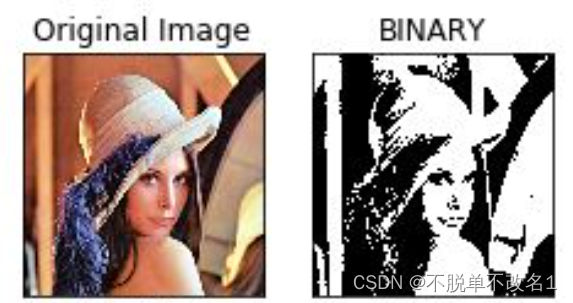
1、二值化图像简介
前面已经完成了摄像头图像的采集和显示,以及RGB图像转灰度图。二值化图像在图像处理领域同样有广泛的应用,本节介绍如何用FPGA实现灰度转二值化图形。灰度实现二值化的原理很简单,只需要设置一个阈值,将每个像素的灰度和阈值比较,大于阈值就输出255,小于阈值就输出0。
2、二值化图像matlab仿真
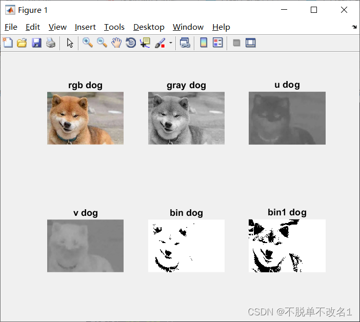
这边简单添加了二值化的matlab代码,代码如下图所示。
clc;
clear all;

img_rgb=imread('dog.png');

%high and width
h=size(img_rgb,1);
w=size(img_rgb,2);

%rgb dog show
subplot(231);
imshow(img_rgb);
title('rgb dog');

% Relized method 2:myself Algorithm realized
% Y = ( R*77 + G*150 + B*29) >>8
% Cb = (-R*44 - G*84 + B*128) >>8
% Cr = ( R*128 - G*108 - B*20) >>8
img_rgb=double(img_rgb);
img_y=zeros(h,w);
img_u=zeros(h,w);
img_v=zeros(h,w);
for i = 1 : h
    for j = 1 : w
        img_y(i,j) = bitshift(( img_rgb(i,j,1)*77 + img_rgb(i,j,2)*150 + img_rgb(i,j,3)*29),-8);
        img_u(i,j) = bitshift((-img_rgb(i,j,1)*44 - img_rgb(i,j,2)*84 + img_rgb(i,j,3)*128 + 32678),-8);
        img_v(i,j) = bitshift(( img_rgb(i,j,1)*128 - img_rgb(i,j,2)*108 - img_rgb(i,j,3)*20 + 32678),-8);
    end
end
img_y = uint8(img_y);
img_u = uint8(img_u);
img_v = uint8(img_v);

% gray to bin
% greater then threshold:1
% smaller than threshold:0
img_bin=zeros(h,w);
img_bin1=zeros(h,w);
THRESHOLD_DATA=80;
THRESHOLD_DATA1=120;
for i=1:h
    for j=1:w
        if(img_y(i,j)>THRESHOLD_DATA)
            img_bin(i,j)=255;
        else
            img_bin(i,j)=0;
        end
        if(img_y(i,j)>THRESHOLD_DATA1)
            img_bin1(i,j)=255;
        else
            img_bin1(i,j)=0;
        end
    end
end

%dog show
subplot(232);
imshow(img_y);
title('gray dog');
subplot(233);
imshow(img_u);
title('u dog');
subplot(234);
imshow(img_v);
title('v dog');
subplot(235);
imshow(img_bin);
title('bin dog');
subplot(236);
imshow(img_bin1);
title('bin1 dog');
最后得到的图像如下图所示。可以看到第五张和第六张图像识二值化后的狗子,第五张图像的阈值是80,第六张图像的阈值是120,可以发现阈值对二值化影响很大,实际应用中应该合理选择阈值。
3、二值化图像FPGA实现
这边编写了gray2bin文件代码来实现灰度到二值化的一个转换,相对应的代码非常简单,如下图所示。
module gray2bin(
    input pclk,
    input rst_n,
    input [23:0] gray_data,
    input gray_data_vaild,
    input gray_clk_en,
    input gray_vsync,

    output wire [23:0] bin_data,
    output wire bin_data_vaild,
    output wire bin_clk_en,
    output wire bin_vsync
);

parameter  THRESHOLD_DATA = 8'd120;

wire [7:0] gray_data0;
reg bin_data0;
reg bin_data_vaild0;
reg bin_clk_en0;
reg bin_vsync0;

assign gray_data0=gray_data[23:16];
assign bin_data_vaild=bin_data_vaild0;
assign bin_clk_en=bin_clk_en0;
assign bin_vsync=bin_vsync0;
assign bin_data={24{bin_data0}};

//Binarization
always @(posedge pclk or negedge rst_n) begin
    if(~rst_n)begin
      bin_data0<=1'b0;
    end
    else if(gray_data0>THRESHOLD_DATA)begin
      bin_data0<=1'b1;
    end
    else bin_data0<=1'b0;
end

//delay 1 tclk
always @(posedge pclk or negedge rst_n) begin
    if(~rst_n)begin
      bin_data_vaild0<=1'b0;
      bin_clk_en0<=1'b0;
      bin_vsync0<=1'b0;
    end
    else begin
      bin_data_vaild0<=gray_data_vaild;
      bin_clk_en0<=gray_clk_en;
      bin_vsync0<=gray_vsync;
    end
end

endmodule
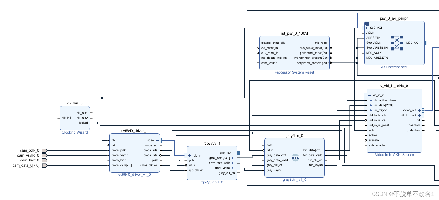
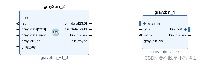
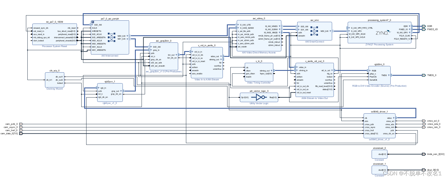
之后我们将它添加到bd中,完成连线如下图所示,因为工程后面连线都一样,所以只截取了前半部分。
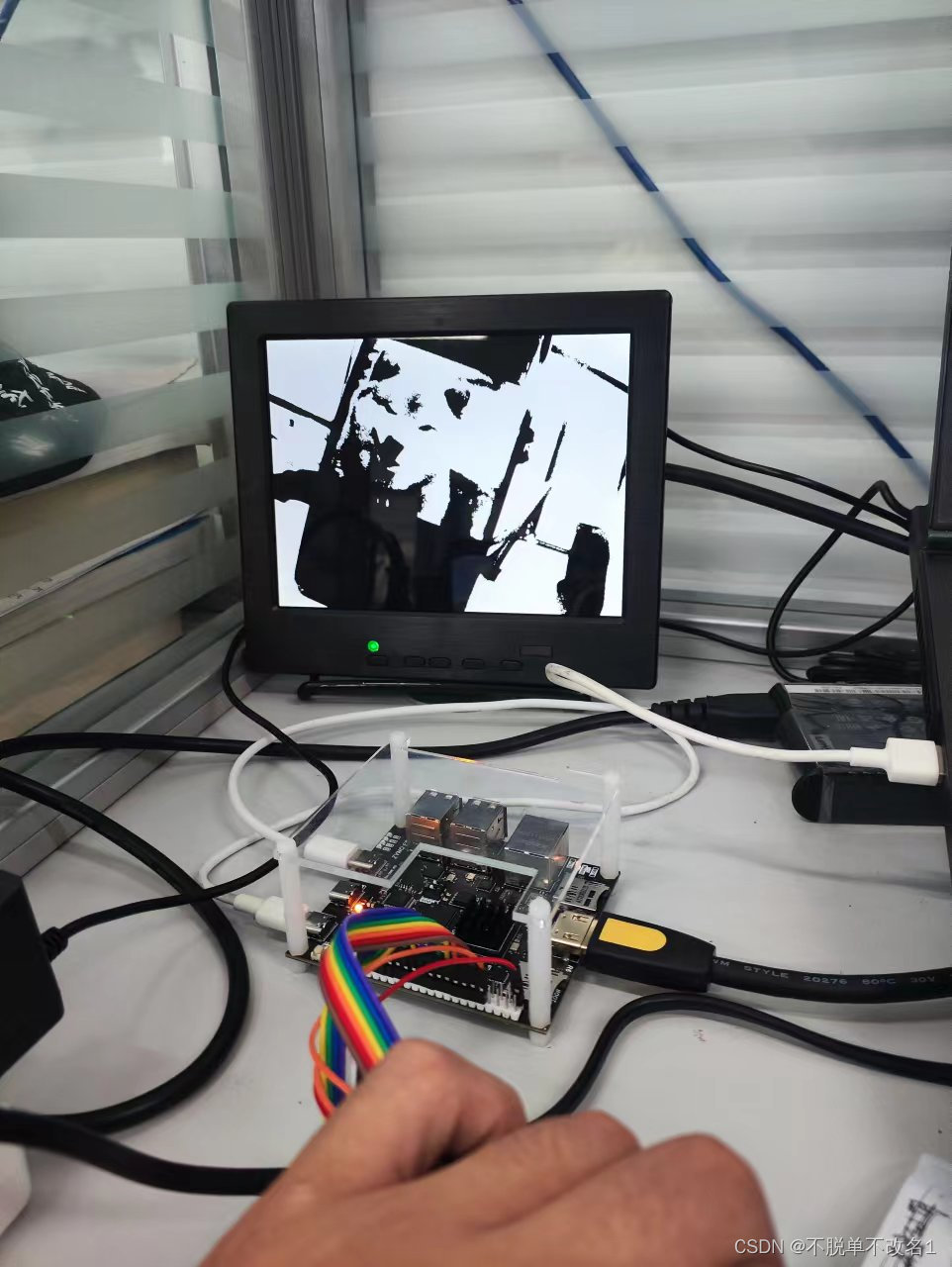
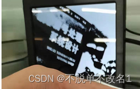
最后导出硬件到sdk进行程序烧写即可查看效果如下图所示。可以发现,二值化受到环境光的影响很严重,不同图像的阈值也不同。
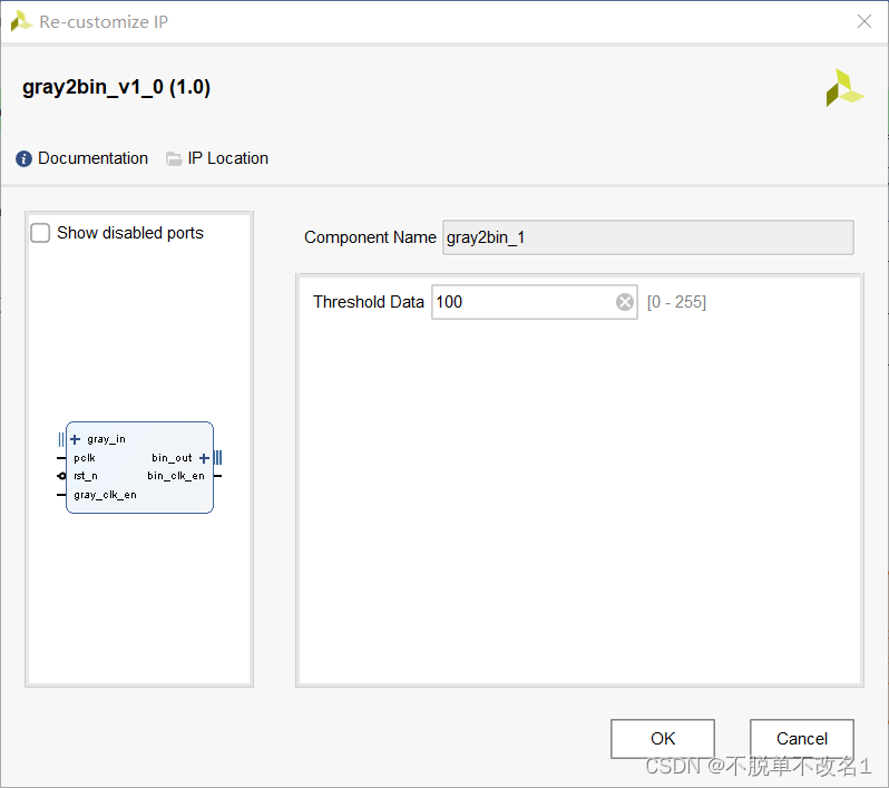
最后将gray2bin这个模块打包成ip核,如下图所示。我们将ip核替换进去后进行连线,最后同样可以得到二值化的图像。
4、ps端控制pl端图像的阈值
虽然在bd图里面可以改变图像的阈值后重新生成bit流,但每次改变阈值就得重新生成硬件,这个过程很繁琐也不方便。想到ZYNQ是带有arm核的,这里便打算封装一个带有axi4接口的二值化ip核,实现ps端对pl端的控制。接下来介绍带有axi接口的二值化模块。
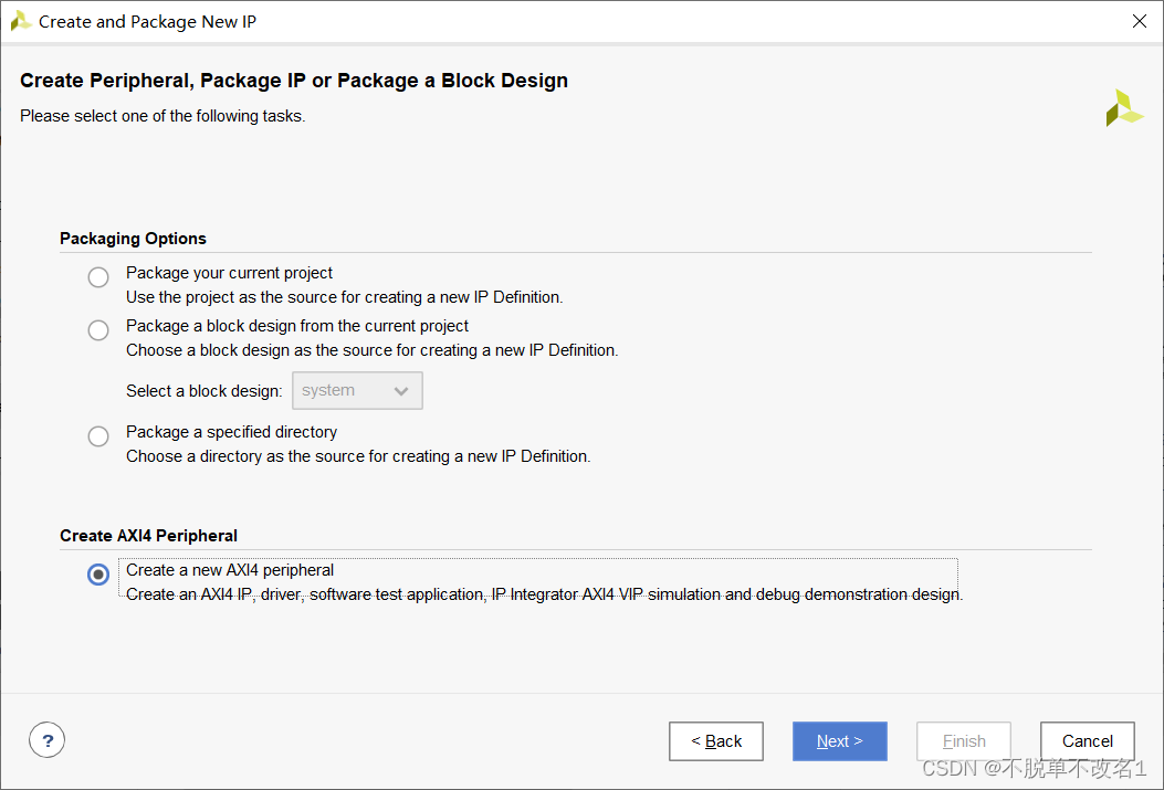
(1)首先第一步是选择tool,选择打包ip,选择打包一个axi4接口的。
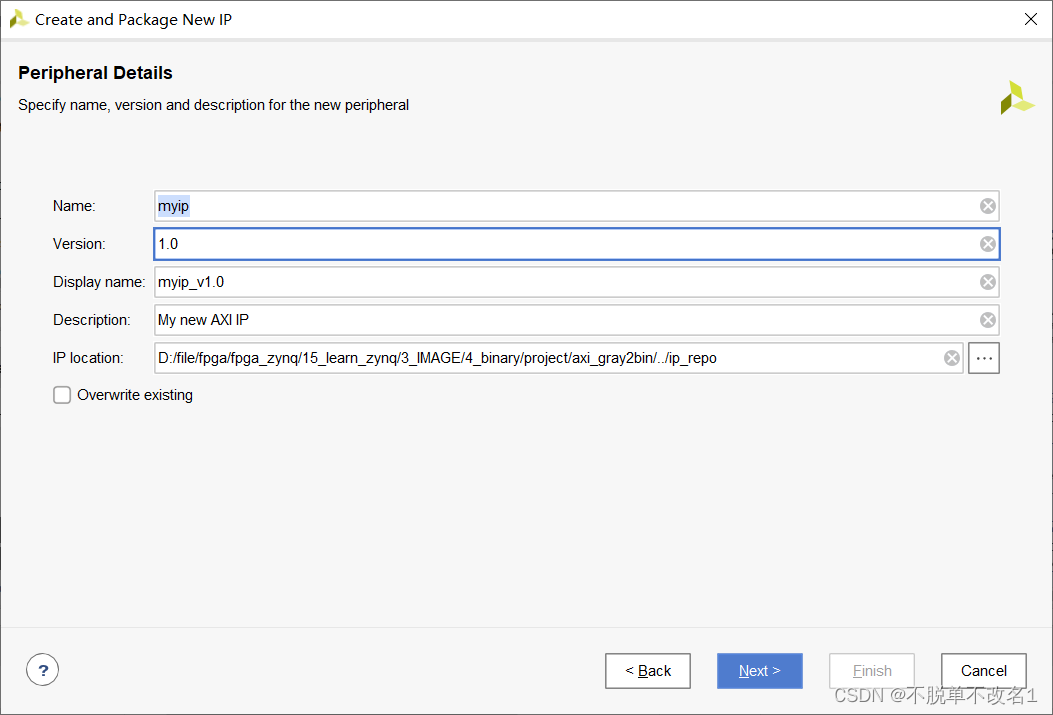
(2)之后是填写ip的相关信息,分别是ip名字、ip版本、ip显示名字、ip描述和ip路径。
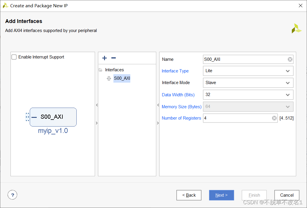
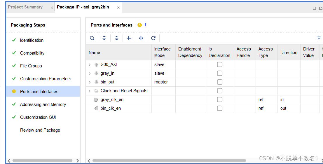
(3)下一个是设置axi接口的相关信息,包括名字、类型、主从模式、位宽以及寄存器个数。
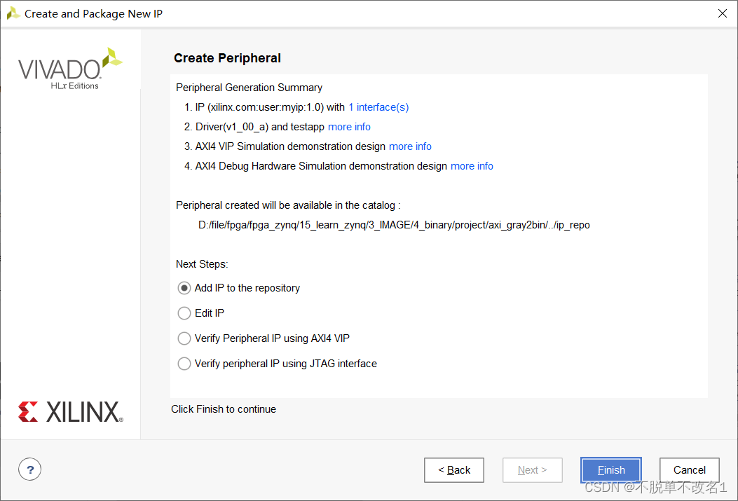
(4)之后将ip添加到工程中
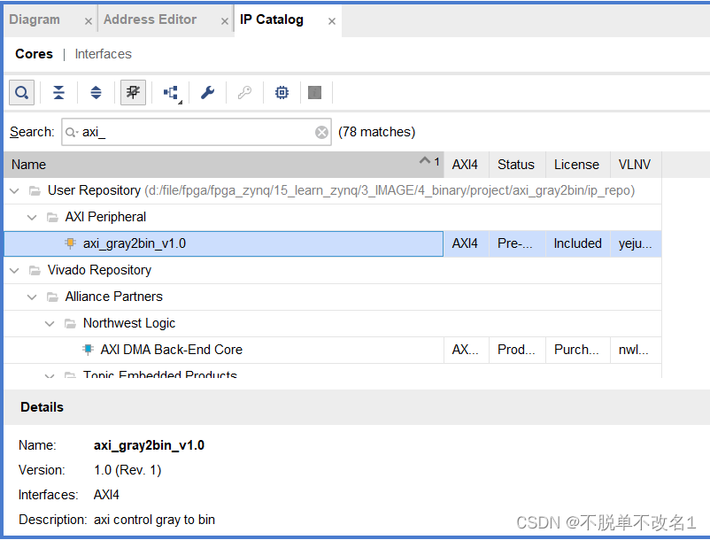
(5)在ip catalog中找到刚刚的ip,右键选择编辑ip核edit in ip packager
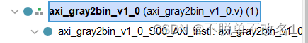
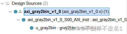
(6)接下来就是比较关键的步骤,这个ip工程自动建立好了之后,会看到生成了这两个.v文件,我们还需要添加一个gray2bin的文件。全部添加好之后如下图所示。
(7)然后是更改接口和例化代码,我这边就之久放代码了,不做过多讲解。
`timescale 1 ns / 1 ps
module axi_gray2bin_v1_0
(
// Users to add parameters here
// User parameters ends
// Do not modify the parameters beyond this line
// Parameters of Axi Slave Bus Interface S00_AXI
parameter integer C_S00_AXI_DATA_WIDTH = 32,
parameter integer C_S00_AXI_ADDR_WIDTH = 4
)
(
// Users to add ports here
input pclk,
input rst_n,
input [23:0] gray_data,
input gray_data_vaild,
input gray_clk_en,
input gray_vsync,
output wire [23:0] bin_data,
output wire bin_data_vaild,
output wire bin_clk_en,
output wire bin_vsync,
// User ports ends
// Do not modify the ports beyond this line
// Ports of Axi Slave Bus Interface S00_AXI
input wire s00_axi_aclk,
input wire s00_axi_aresetn,
input wire [C_S00_AXI_ADDR_WIDTH-1 : 0] s00_axi_awaddr,
input wire [2 : 0] s00_axi_awprot,
input wire s00_axi_awvalid,
output wire s00_axi_awready,
input wire [C_S00_AXI_DATA_WIDTH-1 : 0] s00_axi_wdata,
input wire [(C_S00_AXI_DATA_WIDTH/8)-1 : 0] s00_axi_wstrb,
input wire s00_axi_wvalid,
output wire s00_axi_wready,
output wire [1 : 0] s00_axi_bresp,
output wire s00_axi_bvalid,
input wire s00_axi_bready,
input wire [C_S00_AXI_ADDR_WIDTH-1 : 0] s00_axi_araddr,
input wire [2 : 0] s00_axi_arprot,
input wire s00_axi_arvalid,
output wire s00_axi_arready,
output wire [C_S00_AXI_DATA_WIDTH-1 : 0] s00_axi_rdata,
output wire [1 : 0] s00_axi_rresp,
output wire s00_axi_rvalid,
input wire s00_axi_rready
);
// Instantiation of Axi Bus Interface S00_AXI
axi_gray2bin_v1_0_S00_AXI
.C_S_AXI_DATA_WIDTH(C_S00_AXI_DATA_WIDTH),
.C_S_AXI_ADDR_WIDTH(C_S00_AXI_ADDR_WIDTH)
) axi_gray2bin_v1_0_S00_AXI_inst (
.pclk ( pclk ),
.rst_n ( rst_n ),
.gray_data ( gray_data ),
.gray_data_vaild ( gray_data_vaild ),
.gray_clk_en ( gray_clk_en ),
.gray_vsync ( gray_vsync ),
.bin_data ( bin_data ),
.bin_data_vaild ( bin_data_vaild ),
.bin_clk_en ( bin_clk_en ),
.bin_vsync ( bin_vsync ),
.S_AXI_ACLK(s00_axi_aclk),
.S_AXI_ARESETN(s00_axi_aresetn),
.S_AXI_AWADDR(s00_axi_awaddr),
.S_AXI_AWPROT(s00_axi_awprot),
.S_AXI_AWVALID(s00_axi_awvalid),
.S_AXI_AWREADY(s00_axi_awready),
.S_AXI_WDATA(s00_axi_wdata),
.S_AXI_WSTRB(s00_axi_wstrb),
.S_AXI_WVALID(s00_axi_wvalid),
.S_AXI_WREADY(s00_axi_wready),
.S_AXI_BRESP(s00_axi_bresp),
.S_AXI_BVALID(s00_axi_bvalid),
.S_AXI_BREADY(s00_axi_bready),
.S_AXI_ARADDR(s00_axi_araddr),
.S_AXI_ARPROT(s00_axi_arprot),
.S_AXI_ARVALID(s00_axi_arvalid),
.S_AXI_ARREADY(s00_axi_arready),
.S_AXI_RDATA(s00_axi_rdata),
.S_AXI_RRESP(s00_axi_rresp),
.S_AXI_RVALID(s00_axi_rvalid),
.S_AXI_RREADY(s00_axi_rready)
);
// Add user logic here
// User logic ends
endmodule
`timescale 1 ns / 1 ps
module axi_gray2bin_v1_0_S00_AXI
(
// Users to add parameters here
// User parameters ends
// Do not modify the parameters beyond this line
// Width of S_AXI data bus
parameter integer C_S_AXI_DATA_WIDTH = 32,
// Width of S_AXI address bus
parameter integer C_S_AXI_ADDR_WIDTH = 4
)
(
// Users to add ports here
input pclk,
input rst_n,
input [23:0] gray_data,
input gray_data_vaild,
input gray_clk_en,
input gray_vsync,
output wire [23:0] bin_data,
output wire bin_data_vaild,
output wire bin_clk_en,
output wire bin_vsync,
// User ports ends
// Do not modify the ports beyond this line
// Global Clock Signal
input wire S_AXI_ACLK,
// Global Reset Signal. This Signal is Active LOW
input wire S_AXI_ARESETN,
// Write address (issued by master, acceped by Slave)
input wire [C_S_AXI_ADDR_WIDTH-1 : 0] S_AXI_AWADDR,
// Write channel Protection type. This signal indicates the
// privilege and security level of the transaction, and whether
// the transaction is a data access or an instruction access.
input wire [2 : 0] S_AXI_AWPROT,
// Write address valid. This signal indicates that the master signaling
// valid write address and control information.
input wire S_AXI_AWVALID,
// Write address ready. This signal indicates that the slave is ready
// to accept an address and associated control signals.
output wire S_AXI_AWREADY,
// Write data (issued by master, acceped by Slave)
input wire [C_S_AXI_DATA_WIDTH-1 : 0] S_AXI_WDATA,
// Write strobes. This signal indicates which byte lanes hold
// valid data. There is one write strobe bit for each eight
// bits of the write data bus.
input wire [(C_S_AXI_DATA_WIDTH/8)-1 : 0] S_AXI_WSTRB,
// Write valid. This signal indicates that valid write
// data and strobes are available.
input wire S_AXI_WVALID,
// Write ready. This signal indicates that the slave
// can accept the write data.
output wire S_AXI_WREADY,
// Write response. This signal indicates the status
// of the write transaction.
output wire [1 : 0] S_AXI_BRESP,
// Write response valid. This signal indicates that the channel
// is signaling a valid write response.
output wire S_AXI_BVALID,
// Response ready. This signal indicates that the master
// can accept a write response.
input wire S_AXI_BREADY,
// Read address (issued by master, acceped by Slave)
input wire [C_S_AXI_ADDR_WIDTH-1 : 0] S_AXI_ARADDR,
// Protection type. This signal indicates the privilege
// and security level of the transaction, and whether the
// transaction is a data access or an instruction access.
input wire [2 : 0] S_AXI_ARPROT,
// Read address valid. This signal indicates that the channel
// is signaling valid read address and control information.
input wire S_AXI_ARVALID,
// Read address ready. This signal indicates that the slave is
// ready to accept an address and associated control signals.
output wire S_AXI_ARREADY,
// Read data (issued by slave)
output wire [C_S_AXI_DATA_WIDTH-1 : 0] S_AXI_RDATA,
// Read response. This signal indicates the status of the
// read transfer.
output wire [1 : 0] S_AXI_RRESP,
// Read valid. This signal indicates that the channel is
// signaling the required read data.
output wire S_AXI_RVALID,
// Read ready. This signal indicates that the master can
// accept the read data and response information.
input wire S_AXI_RREADY
);
(中间省略部分代码,不需要做更改)
// Add user logic here
gray2bin u_gray2bin(
.pclk ( pclk ),
.rst_n ( rst_n ),
.gray_data ( gray_data ),
.gray_data_vaild ( gray_data_vaild ),
.gray_clk_en ( gray_clk_en ),
.gray_vsync ( gray_vsync ),
.threshold_data ( slv_reg3[7:0] ),
.bin_data ( bin_data ),
.bin_data_vaild ( bin_data_vaild ),
.bin_clk_en ( bin_clk_en ),
.bin_vsync ( bin_vsync )
);
// User logic ends
endmodule
module gray2bin(
    input pclk,
    input rst_n,
    input [23:0] gray_data,
    input gray_data_vaild,
    input gray_clk_en,
    input gray_vsync,
    input [7:0] threshold_data,

    output wire [23:0] bin_data,
    output wire bin_data_vaild,
    output wire bin_clk_en,
    output wire bin_vsync
);

wire [7:0] gray_data0;
reg bin_data0;
reg bin_data_vaild0;
reg bin_clk_en0;
reg bin_vsync0;

assign gray_data0=gray_data[23:16];
assign bin_data_vaild=bin_data_vaild0;
assign bin_clk_en=bin_clk_en0;
assign bin_vsync=bin_vsync0;
assign bin_data={24{bin_data0}};

//Binarization
always @(posedge pclk or negedge rst_n) begin
    if(~rst_n)begin
      bin_data0<=1'b0;
    end
    else if(gray_data0>threshold_data)begin
      bin_data0<=1'b1;
    end
    else bin_data0<=1'b0;
end

//delay 1 tclk
always @(posedge pclk or negedge rst_n) begin
    if(~rst_n)begin
      bin_data_vaild0<=1'b0;
      bin_clk_en0<=1'b0;
      bin_vsync0<=1'b0;
    end
    else begin
      bin_data_vaild0<=gray_data_vaild;
      bin_clk_en0<=gray_clk_en;
      bin_vsync0<=gray_vsync;
    end
end

endmodule
(8)修改好了代码之后,就是对接口进行一个定义和封装,主要包含了AXI接口、灰度输入接口、二值输出接口、时钟接口、灰度和二值的时钟有效信号。之后就打包ip核。
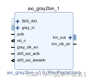
(9)这就是最终打包之后的带有axi接口的灰度转二值化模块了。
(10)将其加入到block design模块中,进行连线得到最终的bd图。然后生成比特流导出硬件即可进行sdk设计。
5、ps端控制pl端图像阈值的软件设计
前面已经得到了带有axi接口的灰度转二值ip核axi_gray2bin。并且设计好了硬件电路。在sdk中新建工程并且添加如下的代码,代码很简单,主要是调用了vivado帮我们生成的读写寄存器函数,对阈值进行读写就可以了。
//宏定义
//frame buffer的起始地址
unsigned int const frame_buffer_addr =0x03000000;
//驱动实例
XAxiVdma vdma;
int main(void)
{
int status;
//配置阈值
AXI_GRAY2BIN_mWriteReg(GRAY2BIN_ADDR, REG3_OFFSET, 0x00000084);
sleep(1);
//配置VDMA
run_vdma_frame_buffer(&vdma, VDMA_ID,WIDTH,HEIGHT,frame_buffer_addr,0,0,BOTH);
status=AXI_GRAY2BIN_mReadReg(GRAY2BIN_ADDR, REG3_OFFSET);
printf("the threshold data is: %d\r\n",status);
return 0;
}
这边测试了下阈值对相同环境同一图像的影响,如下图所示。
(阈值116)

(阈值132)
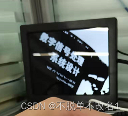
(阈值148)
6、总结
到此为止,摄像头+hdmi显示的环境搭建完成,然后一些基本的图像处理包括RGB2YUV、灰度转二值也做的差不多了。之后会陆续做一些图像的滤波算法、边缘检测、数字识别等。不过要先写我的小论文了!
本文内容由网友自发贡献,版权归原作者所有,本站不承担相应法律责任。如您发现有涉嫌抄袭侵权的内容,请联系:hwhale#tublm.com(使用前将#替换为@)