目录
写在前面
Combinational Logic
Basic Gates
Wire
GND
NOR
Another gate
Two gates
More logic gates
7420 chips
Truth table
Two bit equality
Simple circuit A
Simple circuit B
Combine circuits A and B
Ring or vibrate
Thermostat
3 bit population count
Gates and vectors
Even longer vectors
Multiplexers
2 to 1 mux
2 to 1 bus mux
9 to 1 mux
256 to 1 mux
256 to 1 4bit mux
Arithmetic Circuits
half addr
full addr
3 bit bin addr
addr
signed add over
100 bit bin addr
4 digit BCD addr
Karnaugh Map to Circuit
kamp1
kamp2
kamp3
kamp4
min_SOP
kmap5
kmap6
kmap imple
写在前面
本篇博客对 Circuits 部分的组合逻辑前两节做答案和部分解析,一些比较简单的题目就直接给出答案,有些难度再稍作讲解,每道题的答案不一定唯一,可以有多种解决方案,欢迎共同讨论。
Combinational Logic
Basic Gates
Wire
简单的逻辑实现
module top_module (
    input   in,
    output  out
);
assign out = in;
endmodule
GND
对输出直接接地,言外之意就是将输出置0
module top_module (
    output   out
);
assign out = 1'b0;
endmodule
NOR
实现或非门
module top_module (
    input   in1,
    input   in2,
    output  out
);
assign out = !(in1 | in2);

endmodule
Another gate
module top_module (
    input   in1,
    input   in2,
    output  out
);
assign out = (in1 & (~in2));
endmodule
Two gates
连续的异或操作,中间加入了一个非门
module top_module (
    input   in1,
    input   in2,
    input   in3,
    output  out
);
assign out = (~(in1 ^ in2)) ^ in3;

endmodule
More logic gates
实现各种逻辑门
module top_module(
    input   a, b,
    output  out_and,
    output  out_or,
    output  out_xor,
    output  out_nand,
    output  out_nor,
    output  out_xnor,
    output  out_anotb
);

assign out_and = a & b;
assign out_or = a | b;
assign out_xor = a ^ b;
assign out_nand = ~(a & b);
assign out_nor = ~(a | b);
assign out_xnor = ~(a ^ b);
assign out_anotb = a & (~b);

endmodule
7420 chips
实现 7420 芯片的功能,简单的与非门
module top_module (
    input   p1a, p1b, p1c, p1d,
    output  p1y,
    input   p2a, p2b, p2c, p2d,
    output  p2y
);

assign p1y = ~(p1a & p1b & p1c & p1d);
assign p2y = ~(p2a & p2b & p2c & p2d);

endmodule
Truth table
对真值表进行逻辑实现,这个答案不唯一。
module top_module(
    input   x3,
    input   x2,
    input   x1,
    output  f
);
assign f = x3?x1:x2;

endmodule
Two bit equality
module top_module (
	input [1:0]  A,
	input [1:0]  B,
	output       z
);
assign z = (A == B)? 1:0;

endmodule
Simple circuit A
module top_module (
	input   x,
	input   y,
	output  z
);
assign z = (x ^ y) & x;

endmodule
Simple circuit B
module top_module (
	input   x,
	input   y,
	output  z
);
assign z = ~(x ^ y);

endmodule
Combine circuits A and B
联合前面的电路 A 和 B 的功能,但也可以直接逻辑实现,不必调用之前的模块。
module top_module (
	input   x,
	input   y,
	output  z
);
wire    a1,a2,b1,b2;
wire    sum1,sum2;

assign a1 = (x ^ y) & x;
assign b1 = ~(x ^ y);
assign a2 = (x ^ y) & x;
assign b2 = ~(x ^ y);

assign sum1 = a1 | b1;
assign sum2 = a2 & b2;

assign z = sum1 ^ sum2;

endmodule
Ring or vibrate
设计一个电路来控制手机的振铃器和振动电机。每当电话需要从来电响铃,您的电路必须打开铃声或电机,但不能同时打开两者。如果手机处于振动模式,请打开电机。否则,请打开铃声。
input ring
output ringer = 1
output motor = 1
input vibrate_mode = 1
module top_module (
    input    ring,
    input    vibrate_mode,
    output   ringer,
    output   motor
);

assign ringer = ((ring == 1'b1) && (vibrate_mode == 1'b0))? 1'b1:1'b0;
assign motor = ((vibrate_mode ==1'b1) && (ring == 1'b1))? 1'b1:1'b0;
Thermostat
加热/冷却恒温器控制加热器(冬季)和空调(夏季)。实现一个电路,该电路将根据需要打开和关闭加热器,空调和鼓风机风扇。
恒温器可以处于以下两种模式之一:加热和冷却。在加热模式下,当加热器太冷时打开,但不要使用空调。在冷却模式下,当空调太热时打开,但不要打开加热器。当加热器或空调打开时,也要打开风扇以循环空气。此外,用户还可以要求风扇打开,即使加热器和空调关闭。
mode = 1 mode = 0 too_cold = 1 too_hot = 1 fan_on = 1
尝试仅使用语句,以查看是否可以将问题描述转换为逻辑门的集合。
module top_module (
    input    too_cold,
    input    too_hot,
    input    mode,
    input    fan_on,
    output   heater,
    output   aircon,
    output   fan
);

assign heater = too_cold & mode;
assign aircon = too_hot & ~mode;
assign fan = fan_on | heater | aircon;

endmodule
3 bit population count
“总体计数”电路对输入向量中的'1'的数量进行计数。为 3 位输入矢量构建总体计数电路。
逻辑实现嵌套。
module top_module(
    input  [2:0]  in,
    output [1:0]  out
);

assign out = (in=='d1 | in=='d2 | in=='d4)?'d1:((in=='d3 | in=='d5 | in=='d6)?'d2:((~in)?'d0:'d3));

endmodule
Gates and vectors
在 [3:0] 中,将获得一个四位输入向量。我们想知道每个位与其邻位间的一些关系:
-
out_both:此输出向量的每个位都应指示相应的输入位及其左侧(较高索引)是否均为“1”。例如,out_both[2]应该指示in[2]和in[3]是否都是1。由于in[3]的左边没有邻位,所以我们不需要知道out_both[3]。
-
out_any:此输出向量的每个位都应指示任何相应的输入位及其右侧是否为“1”。例如,out_any[2]应指示[2]或[1]中是否为1。由于 in[0] 没有右边数,所以我们不需要知道out_any[0]。
-
out_different:此输出向量的每个位都应指示相应的输入位是否与其左侧不同。例如,out_different[2]应指示 in[2] 是否与 in[3] 不同。对于这部分,将向量视为环绕,因此在[3]中左邻位在[0]中。
module top_module(
    input   [3:0]   in,
    output  [2:0]   out_both,
    output  [3:1]   out_any,
    output  [3:0]   out_different
);
assign   out_both[0]        =   (in[0] & in[1]);
assign   out_both[1]        =   (in[1] & in[2]);
assign   out_both[2]        =   (in[2] & in[3]);
assign   out_any[1]         =   (in[1] | in[0]);
assign   out_any[2]         =   (in[2] | in[1]);
assign   out_any[3]         =   (in[3] | in[2]);
assign   out_different[0]   =   (in[0] != in[1]);
assign   out_different[1]   =   (in[1] != in[2]);
assign   out_different[2]   =   (in[2] != in[3]);
assign   out_different[3]   =   (in[3] != in[0]);

endmodule
Even longer vectors
和上题类似
module top_module(
    input  [99:0]   in,
    output [98:0]   out_both,
    output [99:1]   out_any,
    output [99:0]   out_different
);

assign out_both[98:0]      = in[99:1] & in[98:0];
assign out_any[99:1]       = in[99:1] | in[98:0];
assign out_different[98:0] = in[98:0] ^ in[99:1];
assign out_different[99]   = in[99] ^ in[0];

endmodule
Multiplexers
2 to 1 mux
创建一个 1 位宽的 2 对 1 多路复用器。当 sel=0 时,选择a。当 sel=1 时,选择 b。
module top_module(
    input   a, b, sel,
    output  out
);
assign out = sel?b:a;

endmodule
2 to 1 bus mux
创建一个 100 位宽的 2 对 1 多路复用器。当 sel=0 时,选择a。当 sel=1 时,选择 b。
module top_module(
    input  [99:0]  a, b,
    input          sel,
    output [99:0]  out
);
assign out = sel?b:a;

endmodule
9 to 1 mux
创建 16 位宽、9 对 1 多路复用器。sel=0 选择 a,sel=1 选择 b,依此类推。对于未使用的情况(sel=9 到 15),请将所有输出位设置为“1”。
module top_module(
    input  [15:0]  a, b, c, d, e, f, g, h, i,
    input  [3:0]   sel,
    output [15:0]  out
);
assign out = (sel=='d0)?a:((sel=='d1)?b:((sel=='d2)?c:((sel=='d3)?d:((sel=='d4)?e:((sel=='d5)?f:((sel=='d6)?g:((sel=='d7)?h:((sel=='d8)?i:16'hffff))))))));

endmodule
256 to 1 mux
创建 16 位宽、9 对 1 多路复用器。sel=0 选择 a,sel=1 选择 b,依此类推。对于未使用的情况(sel=9 到 15),请将所有输出位设置为“1”。
module top_module(
    input  [255:0] in,
    input  [7:0]   sel,
    output         out
);
assign out = in[sel];

endmodule
256 to 1 4bit mux
创建 16 位宽、9 对 1 多路复用器。sel=0 选择 a,sel=1 选择 b,依此类推。对于未使用的情况(sel=9 到 15),请将所有输出位设置为“1”。
module top_module(
    input  [1023:0]  in,
    input  [7:0]     sel,
    output [3:0]     out
);
assign out = in[sel*4+3-:4];

endmodule
Arithmetic Circuits
half addr
创建一个半加法器。半加法器添加两个位(无残留),并产生总和和并执行。
module top_module (
    input  [7:0]  a,
    input  [7:0]  b,
    output [7:0]  s,
    output        overflow
);

assign s = a + b;
assign overflow = (~a[7] & ~b[7] & s[7]) | (a[7] & b[7] & ~s[7]);

endmodule
full addr
创建完整添加器。一个完整的加法器添加三个位,并产生一个总和并执行。
module top_module(
    input   a, b, cin,
    output  cout, sum
);
assign {cout,sum} = a + b + cin;
endmodule
3 bit bin addr
创建3个实例以创建3位二进制纹波携带加法器。加法器将两个3位数字和一个随身数字相加,以生成3位求和并执行。从纹波携带加法器中的每个完整加法器输出执行。cout[2] 是最后一个完整加法器的最终执行。
module top_module(
    input  [2:0]  a, b,
    input         cin,
    output [2:0]  cout,
    output [2:0]  sum
);
assign {cout[0],sum[0]} = a[0] + b[0] + cin;
assign {cout[1],sum[1]} = a[1] + b[1] + cout[0];
assign {cout[2],sum[2]} = a[2] + b[2] + cout[1];

endmodule
addr
做行进波累加器,全加器
module top_module (
    input  [3:0]  x,
    input  [3:0]  y,
    output [4:0]  sum
);

wire    cin1,cin2,cin3;

assign {cin1,sum[0]} = x[0] + y[0];
assign {cin2,sum[1]} = x[1] + y[1] + cin1;
assign {cin3,sum[2]} = x[2] + y[2] + cin2;
assign {sum[4],sum[3]} = x[3] + y[3] + cin3;

endmodule
signed add over
假设有两个 8 位 2 的补码数,a[7:0] 和 b[7:0]。这些数字相加产生s[7:0]。还要计算是否发生了(有符号)溢出。两个正数相加符号位变成了1表示溢出,两个负数相加符号位变成了0表示溢出。
module top_module (
    input  [7:0]  a,
    input  [7:0]  b,
    output [7:0]  s,
    output        overflow
);

assign s = a + b;
assign overflow = (~a[7] & ~b[7] & s[7]) | (a[7] & b[7] & ~s[7]);

endmodule
100 bit bin addr
创建 100 位二进制加法器。加法器将两个 100 位数字和进位相加,以产生 100 位总和。
module top_module(
    input  [99:0]  a, b,
    input          cin,
    output         cout,
    output [99:0]  sum
);
assign {cout,sum} = a+b+cin;

endmodule
4 digit BCD addr
实例化 4 个bcd_fadd模块以创建 4 位 BCD 纹波携带加法器。加法器应添加两个 4 位 BCD 数字(打包成 16 位向量)和进位值,以生成 4 位总和并执行。
module top_module (
    input  [15:0]  a, b,
    input          cin,
    output         cout,
    output [15:0]  sum
);

wire     cin1,cin2,cin3;

bcd_fadd bcd_fadd_inst1(
	.a    (a[3:0]),
	.b    (b[3:0]),
	.cin  (cin),
	.cout (cin1),
	.sum  (sum[3:0])
	);

bcd_fadd bcd_fadd_inst2(
	.a    (a[7:4]),
	.b    (b[7:4]),
	.cin  (cin1),
	.cout (cin2),
	.sum  (sum[7:4])
	);

bcd_fadd bcd_fadd_inst3(
	.a    (a[11:8]),
	.b    (b[11:8]),
	.cin  (cin2),
	.cout (cin3),
	.sum  (sum[11:8])
	);

bcd_fadd bcd_fadd_inst4(
	.a    (a[15:12]),
	.b    (b[15:12]),
	.cin  (cin3),
	.cout (cout),
	.sum  (sum[15:12])
	);

endmodule
Karnaugh Map to Circuit
kamp1
根据卡诺图得出逻辑实现
module top_module(
    input   a,
    input   b,
    input   c,
    output  out
);
assign out = ((~a)&(~b)&(~c))?'d0:'d1;

endmodule
kamp2
根据卡诺图得出逻辑实现
module top_module(
    input   a,
    input   b,
    input   c,
    input   d,
    output  out
);

assign out = (a&~b&c&d)|(~a&b&~c&~d)|(~a&c&~d)|(b&c&d)|(~b&~c);

endmodule
kamp3
根据卡诺图得出逻辑实现
module top_module(
    input   a,
    input   b,
    input   c,
    input   d,
    output  out
);

assign out = (a&~c&~d)|(~b&c)|(a&b&c);
endmodule
kamp4
根据卡诺图得出逻辑实现
module top_module(
    input   a,
    input   b,
    input   c,
    input   d,
    output  out
);

assign out = (~a&b&~c&~d)|(a&~b&~c&~d)|(~a&~b&~c&d)|(a&b&~c&d)|(~a&b&c&d)|(a&~b&c&d)|(~a&~b&c&~d)|(a&b&c&~d);
endmodule
min_SOP
具有四个输入(a,b,c,d)的单输出数字系统在输入端出现2、7或15时生成逻辑-1,当0、1、4、5、6、9、10、13或14出现时,生成逻辑-0。数字 3、8、11 和 12 的输入条件在此系统中永远不会出现。例如,7 对应于分别设置为 0,1,1,1 的 a,b,c,d。确定最小 SOP 形式的输出out_sop,以及最小 POS 格式的输出out_pos。
SOP: sum of product
在卡诺图中标定1的为正,0为反,先乘最后相加
POS: product of sum
在卡诺图中标定1的为反,0为正,先加最后相乘再取反
module top_module (
    input    a,
    input    b,
    input    c,
    input    d,
    output   out_sop,
    output   out_pos
);
assign out_sop = (~a&~b*c) | (c&d);
assign out_pos = ~((a|b|~c) & (~c|~d));

endmodule
kmap5
根据卡诺图得出逻辑实现
module top_module (
    input [4:1]  x,
    output       f
);
assign f = (~x[1]&x[3]) | (x[1]&x[2]&~x[3]);

endmodule
kmap6
根据卡诺图得出逻辑实现
module top_module (
    input [4:1]  x,
    output       f
);
assign f = (~x[1]&x[3]) | (x[1]&~x[2]&~x[4]) | (x[1]&x[2]&x[3]&x[4]) | (~x[1]&~x[2]&~x[3]&~x[4]);

endmodule
kmap imple
对于下面的Karnaugh图,使用一个4对1多路复用器和尽可能多的2对1多路复用器来提供电路实现,但使用尽可能少。您不得使用任何其他逻辑门,必须使用 a 和 b 作为多路复用器选择器输入,如下面的 4 对 1 多路复用器所示。
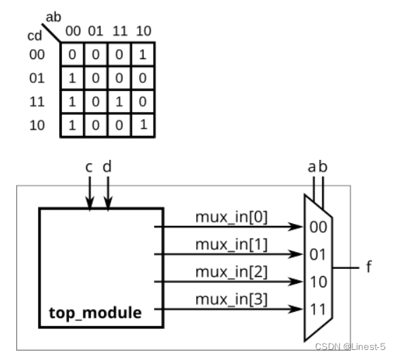
module top_module (
    input         c,
    input         d,
    output [3:0]  mux_in
);
assign mux_in[0] = c | d;
assign mux_in[1] = 'd0;
assign mux_in[2] = ~d;
assign mux_in[3] = c & d;
endmodule